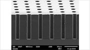
Toray developed a negative photosensitive polyimide material that is 100 micrometers thick and can fabricate vias with 10 micrometer diameters.
Toray Industries announced that it has developed a negative photosensitive polyimide material. This new offering maintains the characteristic thermal resistance, mechanical properties, and adhesiveness of polyimides while increasing resolutions and enabling high-definition pattern formation on 100-micrometer and other thick films.
The number of electronic components in smartphones and other mobile devices will increase to accommodate the greater speeds and capacities of 5G, 6G, and subsequent broadband cellular networks. These devices will need more miniaturized electronic components and higher density mountings. Finer fabrication processes for polyimide materials will thus be necessary for the insulating layers of electronic components.
Toray developed a negative photosensitive polyimide material that is 100 micrometers thick and can fabricate vias with 10 micrometer diameters. The company achieved this by leveraging the functional polyimide design technology it has amassed over the years to enhance light transmittance and control photoreactions.
Toray additionally made it possible to cut thermal stress to less than half that of regular polyimide materials and thus reduce warping by controlling polyimide resin cross-linking density from photoreactions during exposure and lowering curing shrinkage.
This material should make it possible to miniaturize electronic components and semiconductor package wiring and enhance reliability. Toray is shipping prototypes with a view to commercializing the material as a varnish and sheet.
The company aims to augment its lineup with grades with low thermal expansion coefficients and dielectric levels and small dielectric losses, offering them for semiconductor devices and electronic components that can drive ultrafast communication technologies.
Subscribe to our newsletter & stay updated.