As semiconductor complexity rises, advanced analytical solutions are becoming critical to maintaining purity, performance, and yield
As the semiconductor industry advances toward smaller nodes and more complex architectures, the demand for ultra-pure materials and precise contamination control has intensified. Among these, Inductively Coupled Plasma Mass Spectrometry (ICP-MS) stands out for its ability to detect elements at parts-per-trillion levels with exceptional accuracy.
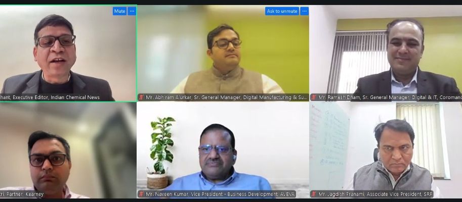
Recently experts discussed how ICP-MS is enabling laboratories to meet the stringent purity requirements at the e-Conference titled “Semiconductor Purity: The Power of ICP-MS and Advanced Analytical Techniques.” organized by Indian Chemical News (ICN) in association with PerkinElmer, a global analytics services and solutions provider for the biopharma, food, environmental, safety and applied end markets.
The discussion held on April 22, 2026 was moderated by Pravin Prashant, Executive Editor, ICN who emphasised the increasing demands on analytical laboratories to deliver ultra-precise, highly sensitive, and reliable measurement capabilities.
“As device architectures shrink and materials grow more complex, the need for ultra-trace element analysis has never been greater,” outlined Prashant.
Sunil Nair, Country Marketing Head, India & South Asia, PerkinElmer, said, “One of the defining aspects of PerkinElmer is its strong emphasis on innovation and understanding customer needs and delivering solutions tailored to those requirements. India plays a critical role in our global strategy. We have established a Center of Excellence in Mumbai and, in 2024, launched a global R&D center with over 100 professionals focusing on software and IT capabilities. We continue to expand our portfolio with new launches such as the NexION 1100 ICP-MS, Pyris 9 thermal systems, and advanced LC-MS/MS and IR microscopy technologies. More innovations are planned in the coming years.”
Speaking on the customer support services offered by PerkinElmer, Nairinformed: “Our operations are structured across five global business lines including analytical solutions, customer enablement, genomics and proteomics, OneSource services, and food solutions. Today, a significant portion of our focus is on analytical solutions and customer support. We have strengthened our customer enablement team, with more than 85 service engineers across India and an installed base of over 14,000 systems, ensuring timely support nationwide. We remain committed to evolving alongside our customers and delivering better solutions through continuous innovation.”
Dheeraj Sinha, DGM, Spectroscopy & Inorganic Product Line Leader, PerkinElmer, said, “The semiconductor market is currently valued at around $45 billion and is expected to grow to nearly $100 billion, driven by a CAGR of about 13%. This momentum is fueled by technological advancements, government initiatives like the India Semiconductor Mission and PLI schemes, and increasing global partnerships. We have a strong foundation with a deep pool of engineering talent, a robust IT base, and growing R&D capabilities. At the same time, there are limitations such as dependence on foreign technology, infrastructure gaps, high capital investment requirements, and a shortage of specialized skills.”
Highlighting PerkinElmer’s capabilities, Sinha added: Trace metal analysis is critical, often requiring detection at parts-per-trillion levels, where ICP-MS becomes indispensable. Organic contaminants are analyzed using FTIR and GC-MS, while thermal properties are studied using DSC, TGA, and DMA. We offer a comprehensive portfolio covering inorganic analysis through ICP-MS and ICP-OES, organic analysis through GC-MS, and thermal and spectroscopic techniques for complete semiconductor characterization. As semiconductor processes become more advanced, the demand for ultra-sensitive, reliable analytical techniques will continue to grow, making technologies like ICP-MS central to the industry.”
P. V. G. Menon, Vice President & Head, Business Development, Advanced Technology Facilities, Tata Projects Limited said, “The global electronics industry is already massive and expected to reach trillions of dollars in the next few years. The semiconductor market itself is rapidly expanding alongside it. India has been working towards building semiconductor capabilities for many years, and now we are seeing real momentum. With initiatives like digital identity, mobile penetration, and increased device usage, the demand for semiconductor components has grown significantly.”
The semiconductor value chain is highly complex, involving materials, capital equipment, design software, fabrication, assembly, and final product integration. Fabrication facilities require extremely controlled environments, cleanrooms with strict limits on contamination, temperature, humidity, and even airborne particles. While India produces a large number of engineers, the semiconductor industry requires highly specialized skills. We expect the workforce demand to double in the next few years. Beyond technical skills, the industry requires discipline and precision. This is not an environment where a mere good enough approach works,” added Menon while emphasising the need for mindset change.
Ashutosh Bhave, Founder & CEO, 14Si Solutions said, “At its core, contamination is simple, meaning anything that should not be present in a given material or process is considered a contaminant.” If we delve deeper, there are few that are very important. Firstly, metals are critical and must be monitored across all materials, including gases and chemicals. Secondly, particles can originate from virtually anywhere, including the environment and manufacturing systems. Thirdly, organic contaminants are often complex and difficult to detect, especially in advanced formulations. Even trace levels of contamination can cause significant damage, including device failure or reduced performance.”
Highlighting the need for a balanced approach while selecting the analytical methods, Bhave added further: “Contaminants are introduced across the entire ecosystem, from raw material sourcing to processing and handling. Detecting these impurities is extremely complex and requires advanced techniques, deep expertise, and continuous learning. Certain chemicals, such as sulfuric acid or mixed formulations, create significant analytical challenges due to interference effects in ICP-MS. Each matrix behaves differently, and there is no single solution. Scientists must understand the chemistry deeply and adapt analytical methods accordingly.”
Subscribe to our newsletter & stay updated.







,_Aditya_A__Shriram_(President).JPG)