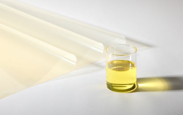
PID is a photosensitive dielectric material used to form ultra-fine interconnects between semiconductor chips and substrates
LG Chem announced that it has successfully developed a proprietary liquid photo-imageable dielectric (PID), a key material for advanced semiconductor packaging, and is now accelerating its efforts to meet the growing demand in artificial intelligence (AI) and other high-performance semiconductor markets.
PID is a photosensitive dielectric material used to form ultra-fine interconnects between semiconductor chips and substrates. By enabling precise electrical pathways and improving circuit fidelity, PID enhances both performance and reliability in advanced packaging processes. As the need for denser and more complex circuitry continues to rise with next-generation semiconductors, demand for high-performance PID materials has grown significantly.
LG Chem’s newly developed liquid PID delivers high-resolution patterning with low-temperature curing, while offering low shrinkage and minimal moisture absorption for improved process stability. Importantly, the material is free of per- and polyfluoroalkyl substances (PFAS) and excludes organic solvents such as N-methyl-2-pyrrolidone (NMP) and toluene, ensuring compliance with increasingly strict global environmental regulations.
In addition to liquid PID, LG Chem has completed development of a film-type PID optimized for advanced IC substrates. Building on its deep expertise in film technologies across displays, semiconductors, and automotive electronics, the company is collaborating with leading global semiconductor manufacturers to bring this innovation to market. Unlike conventional liquid PID, which faces challenges in double-sided application and uniform coating on larger panels, LG Chem’s film PID is supplied as an attachable film that maintains consistent thickness and pattern fidelity across large substrates. Its high strength, elasticity, and low moisture absorption reduce the risk of cracking under repeated thermal cycling. Furthermore, the material is fully compatible with existing lamination equipment, enabling substrate makers to adopt the technology without additional process modifications.
“LG Chem is proactively addressing our customers’ needs for advanced packaging innovation across a broad materials portfolio,” said LG Chem CEO Shin Hak-cheol. “We are committed to going beyond material supply to shape new industry trends in partnership with our customers.”
By expanding its portfolio of advanced packaging materials—including Copper-Clad Laminate (CCL), Die Attach Film (DAF), Non-Conductive Film (NCF), and Build-Up Film (BUF)—LG Chem is reinforcing its position as a global leader in semiconductor materials innovation.
Subscribe to our newsletter & stay updated.