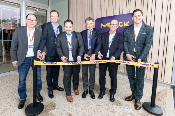
Merck KGaA, Darmstadt has inaugurated a new Metrology & Inspection facility in Saint-Ismier, France, marking a major expansion of its semiconductor technology footprint as global demand for high-performance chips surges.
The €20 million, 4,500 m² site—located in the Grenoble semiconductor cluster—significantly boosts the company’s ability to develop and manufacture precision inspection tools critical for next-generation chip production, particularly as AI accelerates industry demand.
“Advancing chip performance increasingly relies on the intricate architecture of chip systems rather than solely on miniaturization. With chip designs becoming increasingly complex, even the smallest inconsistencies can jeopardize entire systems.
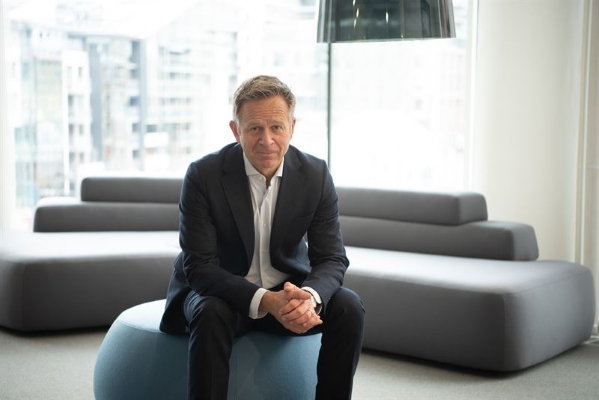
"This makes quality assurance and reliability more challenging than ever,” said Ben Hein, Member of the Executive Board of Merck KGaA, Darmstadt, Germany, and CEO Electronics.
“Our expertise in metrology and inspection provides chip manufacturers with the precise tools and solutions they need to realize the next wave of technological advancements.”
The new site increases Merck KGaA, Darmstadt, Germany’s Metrology & Inspection production capacity fivefold, strengthening its role in advanced packaging and heterogeneous integration—key technologies that stack memory and logic chips vertically to boost performance while reducing energy use.
Metrology systems at the facility measure critical parameters such as depths, step heights, and thicknesses, enabling real-time process adjustments. Inspection tools detect microscopic defects to ensure manufacturing precision. Together, they are designed to improve yields, cut costs, and speed up production cycles for advanced semiconductors.
The Electronics division remains central to the company’s growth strategy. The October 2024 acquisition of Unity-SC in Montbonnot-Saint-Martin further expanded its optical capabilities, reinforcing its push into high-end chip inspection technologies.
With more than 100 employees already on site—and plans to add around 100 more advanced engineering roles over the next four years—the facility will support applications across AI, High-Performance Computing (HPC), and High-Bandwidth Memory (HBM), underscoring the company’s focus on long-term semiconductor growth.
Sustainability is also embedded in the design. The building features a straw-insulated wooden structure, a hermetic concrete base, and rooftop photovoltaic panels along with solar canopies, supplying roughly 40% of its energy needs.
Inside, energy-efficient systems including adjustable sunshades and underfloor cooling and heating are designed to reduce environmental impact while improving workspace comfort.