Fujifilm’s semiconductor materials business has nearly doubled in sales from FY2021 to FY2024
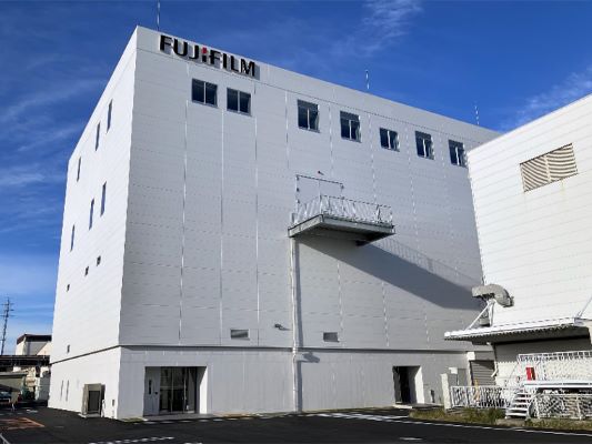
Japan's Fujifilm Corporation has unveiled a state-of-the-art development and evaluation building at its Shizuoka Factory, a major step in expanding its semiconductor materials business. Operations at the new facility began this month.
The investment boosts Fujifilm’s capabilities in performance and quality evaluation, speeding up the development of advanced and next-generation semiconductor materials while ensuring a stable supply of high-quality products. The move comes as demand for semiconductors powering AI, 5G, and IoT continues to surge globally.
Fujifilm’s semiconductor materials business has nearly doubled in sales from FY2021 to FY2024 and is now a core driver of the group’s growth. To support this expansion, the company invested over ¥100 billion in facilities from FY2021 to FY2024 and plans another ¥100 billion+ from FY2025 to FY2026.
The new Shizuoka building features high-cleanliness cleanrooms, cutting-edge evaluation equipment, and AI-powered inspection systems that detect microscopic particles, enhancing analysis accuracy and quality control.
A dedicated digital transformation (DX) department will further integrate AI and digital technologies into manufacturing processes. For business continuity, the building incorporates an RC column-head seismic isolation structure and situates the cleanroom 12 meters above ground to mitigate flooding risks.
The Shizuoka Factory works closely with Fujifilm’s global R&D and production bases, supporting next-generation process technologies worldwide. With the new facility, Fujifilm aims to accelerate the development of advanced EUV, ArF, NIL, PFAS-free materials, and its flagship Wave Control Mosiac technology, cementing its role in the future of semiconductors.
Subscribe to our newsletter & stay updated.